Global semiconductor growth and the future of advanced manufacturing
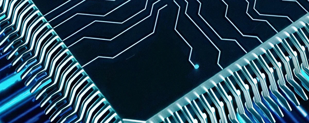
The semiconductor sector is expanding rapidly as chips become increasingly important across AI, high-performance computing, electric mobility, telecommunications, data centres and consumer electronics. This growth is driving substantial investments in new fabrication plants and manufacturing capacity across India and major global markets. At the same time, technological advancements in chip miniaturisation, 3D integration and advanced packaging are making manufacturing processes more sophisticated. These developments are increasing the need for highly controlled production environments, ultra-pure water, reliable utilities and efficient water and wastewater management systems.
Semiconductor manufacturing: from silicon to integrated circuits
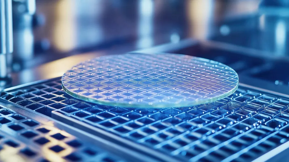
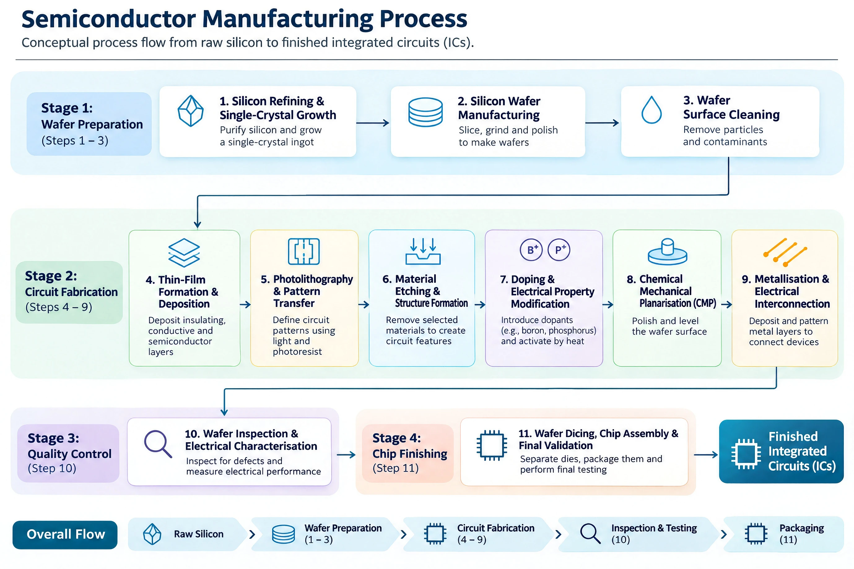
Semiconductor manufacturing involves a sequence of precision processes that transform high-purity silicon into functional integrated circuits (ICs). The process includes wafer preparation, circuit fabrication, electrical testing, chip separation and packaging.
 01
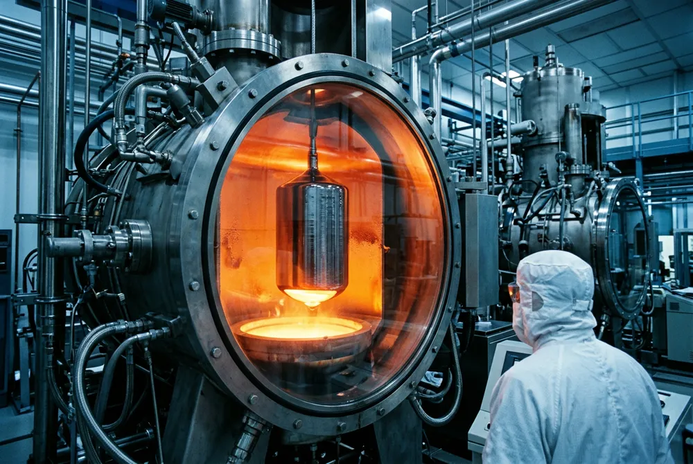
Silicon refining and single-crystal growth
Silicon is extracted from silica-rich materials and purified to remove impurities. The refined silicon is melted and grown into a single-crystal ingot, typically using the Czochralski process.
 02
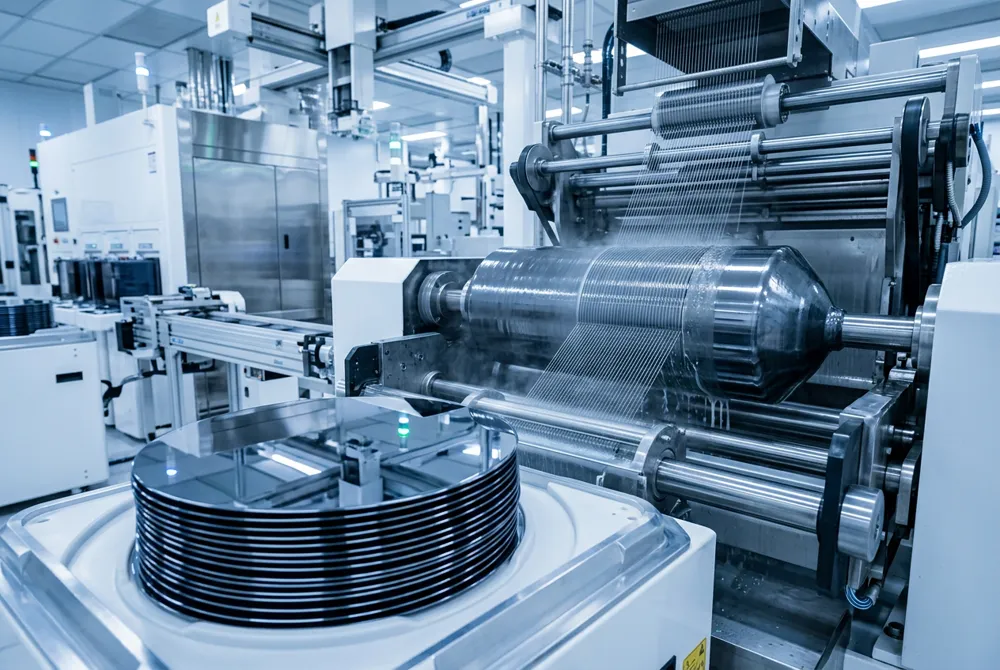
Silicon wafer manufacturing
The single-crystal ingot is sliced into thin circular wafers, followed by grinding, lapping and polishing to achieve the required thickness, dimensions and surface smoothness.
 03
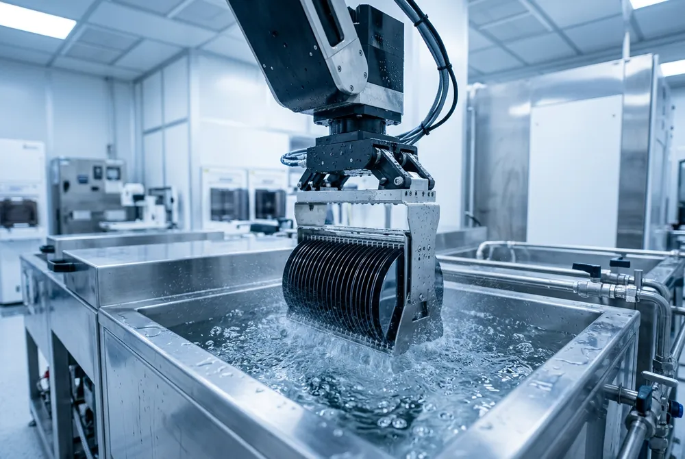
Wafer surface cleaning
Wafers undergo specialised chemical cleaning and ultra-pure water rinsing to remove particles, organic residues, metallic contaminants and other impurities before fabrication.
 04
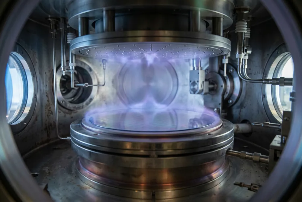
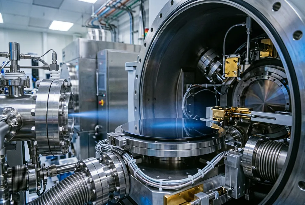
Thin-film formation and deposition
Thin insulating, conductive and semiconductor layers are deposited onto wafers using techniques such as Chemical Vapour Deposition (CVD), Physical Vapour Deposition (PVD) and Atomic Layer Deposition (ALD).
 05
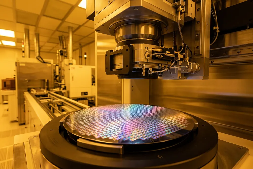
Photolithography and pattern transfer
A light-sensitive photoresist coating is applied to the wafer and exposed through patterned masks. After development, the resulting patterns define the microscopic circuit structures.
 06
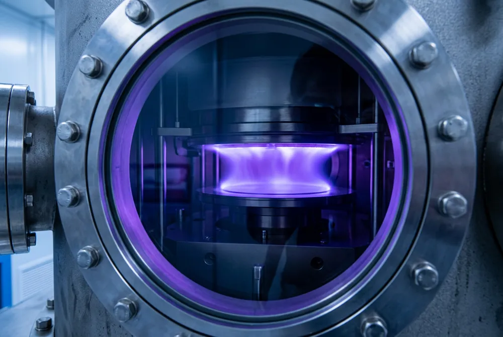
Material etching and structure formation
Selected material layers are selectively removed using wet chemical or plasma-based dry etching to create the required circuit features and structures.
 07
Doping and electrical property modification
Controlled quantities of dopants, such as boron and phosphorus, are introduced into specific wafer regions through ion implantation, followed by heat treatment to establish the desired electrical properties.
 08
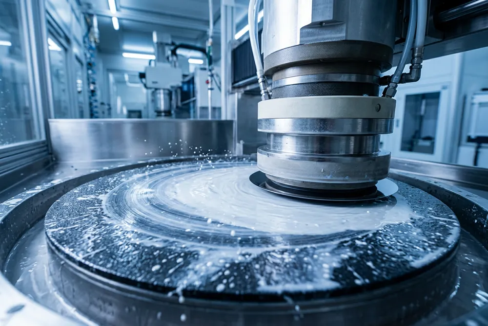
Chemical mechanical planarisation (CMP)
Chemical and mechanical polishing processes remove excess material and create smooth, uniform wafer surfaces for subsequent fabrication steps.
 09
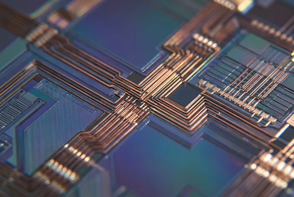
Metallisation and electrical interconnection
Conductive materials, such as copper and aluminium, are deposited and patterned to establish electrical connections between transistors and other circuit components.
 10
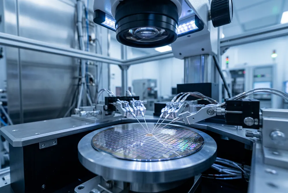
Wafer inspection and electrical characterisation
Advanced inspection and measurement systems identify fabrication defects and assess circuit quality. Electrical probing evaluates individual dies before packaging.
 11
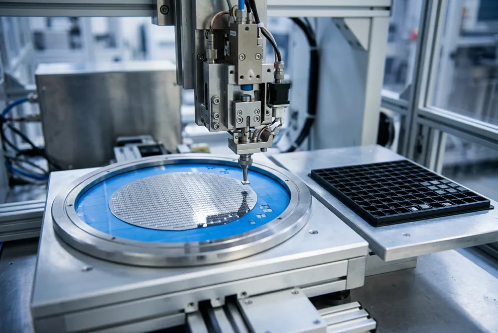
Wafer dicing, chip assembly and final validation
The completed wafer is separated into individual dies, which are assembled, electrically connected and encapsulated. Final electrical and reliability testing ensures that packaged chips meet performance specifications.
Semiconductor manufacturing process: silicon to integrated circuits
Solutions offering for semiconductor industry
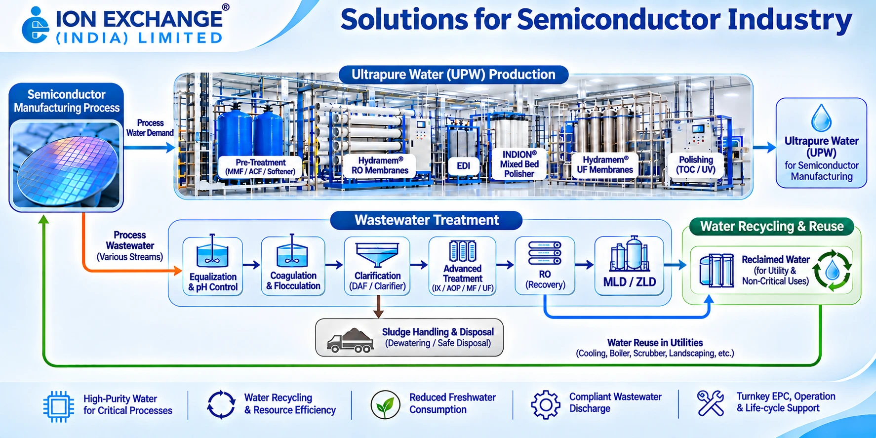
Ion Exchange India Ltd. delivers integrated water and wastewater management solutions tailored to the demanding requirements of the semiconductor industry. Semiconductor manufacturing requires ultra-high-purity water, stringent contamination control and reliable water availability across complex production processes. High water and energy consumption, chemically complex wastewater and stringent operational requirements further increase the need for efficient and sustainable water management. Maximising water recovery and recycling while minimising freshwater consumption and environmental impact is therefore essential.
Our technology portfolio encompasses ultrafiltration, reverse osmosis, electro-deionisation, ion exchange, ultrapure water polishing, effluent treatment, water recycling and Zero Liquid Discharge (ZLD) systems. These solutions cater to critical manufacturing applications, including chemical mechanical planarisation (CMP), wafer cleaning, etching, stripping, metallisation and low-TDS rinsing.
Semiconductor industry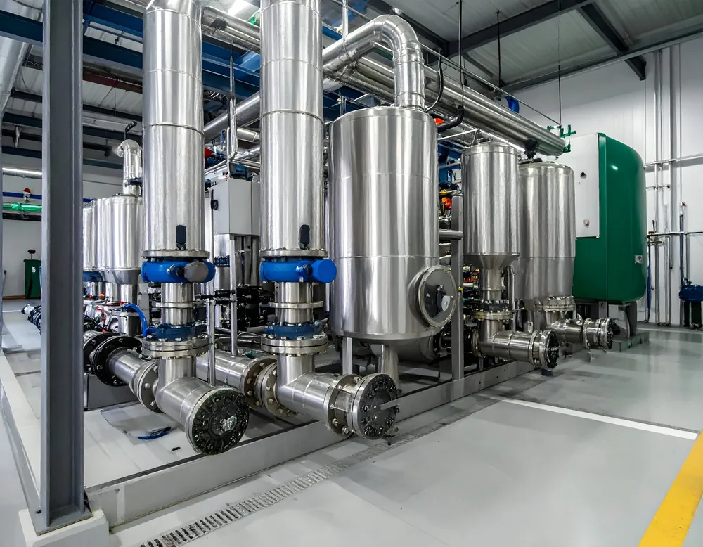
Key solutions offerings
| No. | Key solutions | Ion Exchange (India) Ltd offering |
|---|---|---|
| 1 | Ultrapure Water (UPW) Generation | RO / double-pass RO, EDI, INDION ion-exchange and mixed-bed polishing, UV oxidation, degasification and final filtration. |
| 2 | Process & Utility Water Treatment | HYDRAMEM UF / RO, softening, demineralisation, and cooling- and boiler-water treatment. |
| 3 | Semiconductor Effluent Treatment | Segregated treatment of CMP, acidic / alkaline, fluoride-bearing and metal-containing streams using physicochemical treatment, precipitation, filtration, biological treatment and membrane processes, as applicable. |
| 4 | Advanced Water Recycling & Reuse | HYDRAMEM UF / NF / RO and integrated high-recovery membrane systems to recover treated wastewater for suitable utility and process-water reuse. |
| 5 | Zero Liquid Discharge (ZLD) | Membrane brine concentration, along with thermal solutions (evaporation and crystallisation) for water recovery and minimised liquid discharge. |
| 6 | Digital Monitoring & Plant Optimisation | IONSiTE digital solutions, online water-quality monitoring, process automation and performance optimisation for water, energy and plant reliability. |
Get in touch
Connect with our experts to explore advanced, reliable and sustainable water treatment and process solutions for the semiconductor industry.